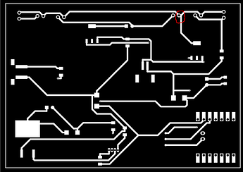
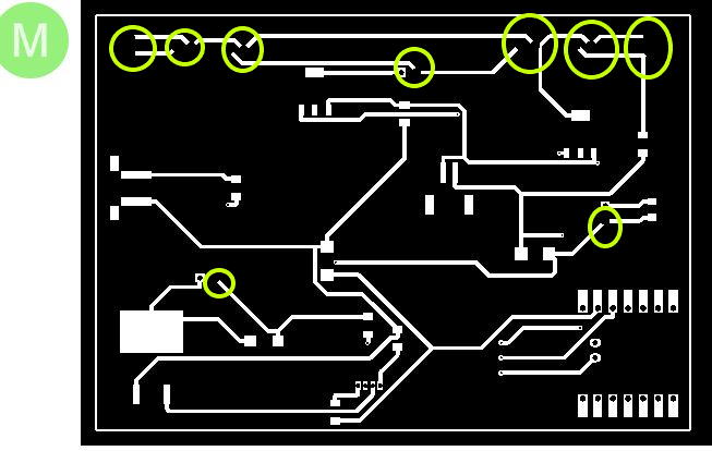
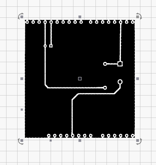
Notice you might have some hickups on your original image and SVG.
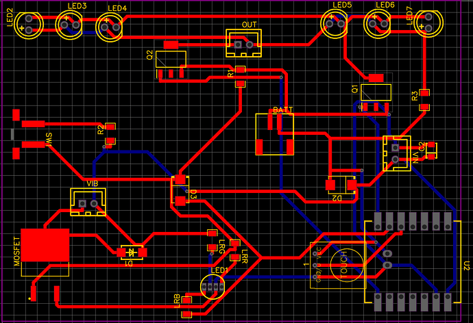
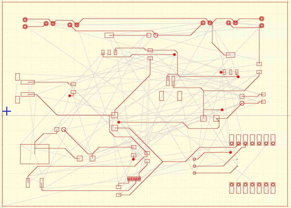
Agreed that does look like hiccups, because it doesn’t include the bottom layer or the top silk or all the pads, at the time I was just trying for the basics on the top layer to get started.
Thanks for your help!
Perhaps if EasyEDA can put the tracks in the same layer as the pads after the Inkscape Stroke to Path everything becames fine…
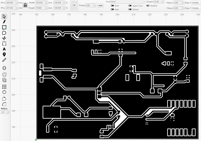
I was curious to see what would happen if I opened it in another app. and it looks like it might work without jumping through hoops.
I found that exporting my PCB to Affinity2 and then flattening the layers and then exporting it to a PDF I can then open it in light burn and print the PCB correctly.
Thanks for all your help and suggestions, they got me on the right path.
This topic was automatically closed 30 days after the last reply. New replies are no longer allowed.
