Hey Karl,
I spend a lot of time designing PCBs in KiCad for my day job, including doing all sorts of weird stuff no one else should be doing (aspirations for PCB designs generated by code, a coworker writing a 13,000 line rust library to parse and manipulate the KiCad file format to make changes to lots and lots of boards at once, scripts and pipelines to create exports of CAD Models, gerbers, graphics of our PCB designs…)
Anyways, I have been thinking about your problem and I suggest you try playing with tracespace view
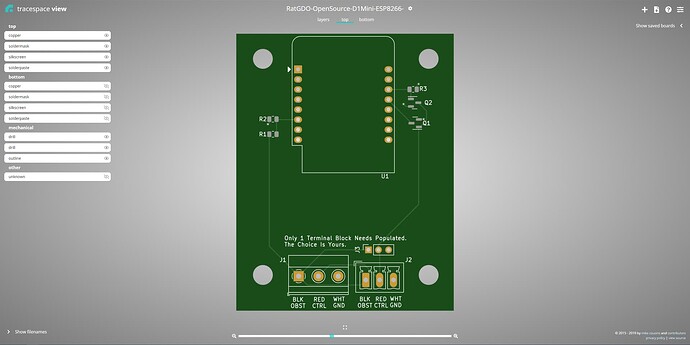
Here is a tracespace render of the gerbers of an open source board I was looking at a while ago. You would just export standard gerbers from KiCad and feed them in here.
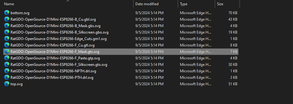
Now, I will use the download button in the top right corner, and I get a bunch of SVG files, one for each layer, as well as a combined graphical but still vector SVG render of the top and bottom of the board.
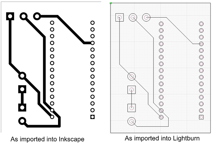
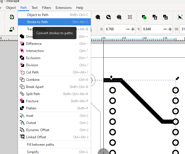
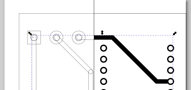
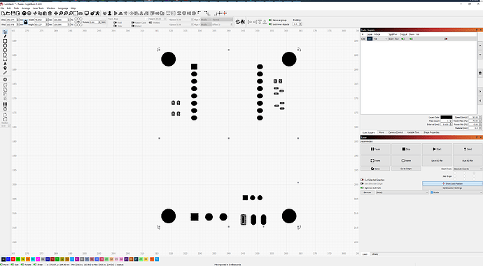
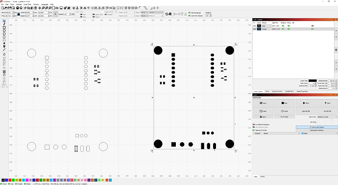
LB doesn’t like this SVG, so I went ahead and ran it through here. I didn’t change the size or anything:
Here you go.
It’s not perfect, as some of the “oval” shapes have internal geometry that needs to be removed, but a few minutes with snipping tools would be better than the advanced custom drawing you’d have to do before.
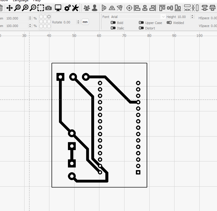
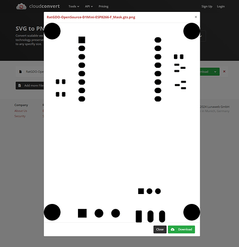
Alternatively, you could convert the original SVG to PNG at a high DPI:
And there you go, that should be ready to run.
I have spent a lot of time working on tangentially related problems that use this same tooling 
Another benefit here is that if this flow works well for you, it is possible to script and automate it, everything from the “creating the gerbers in kicad” to “using the tracespace open source libraries to create these SVG’s” to “using another library to convert them to PNG which you can use in LB”.
