I did not even get this close playing with DPI. I tried Trace and went thru a learning curve that ended in nothing better.
1 Like
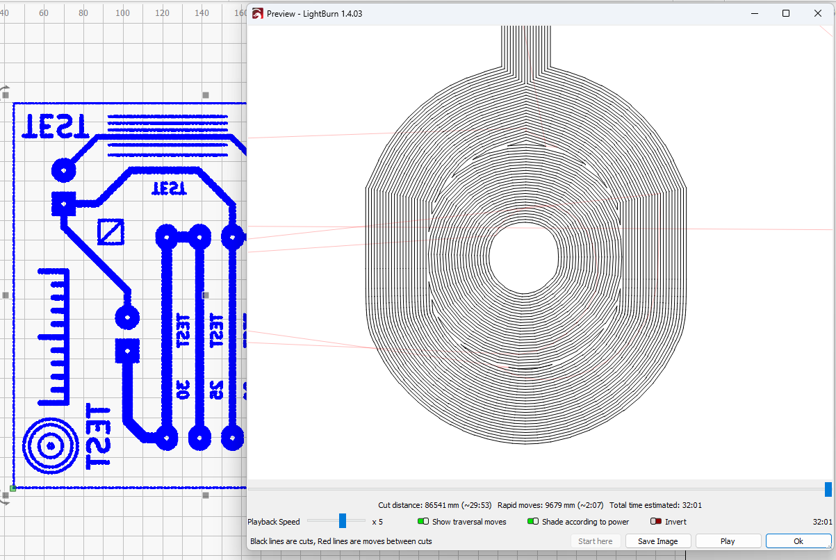
Ok I think we got there ! and a big thanks to everyone that made time to assist me with great helpful comments. I think maybe John got there first with the scanning offset being the main issue. I watched the Lightburn tutorial on Youtube and followed the offset tuning method which I have done from 500 - 10,000mm in 500mm steps.

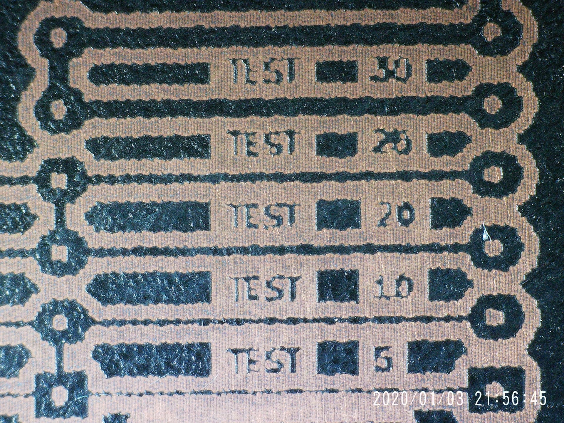
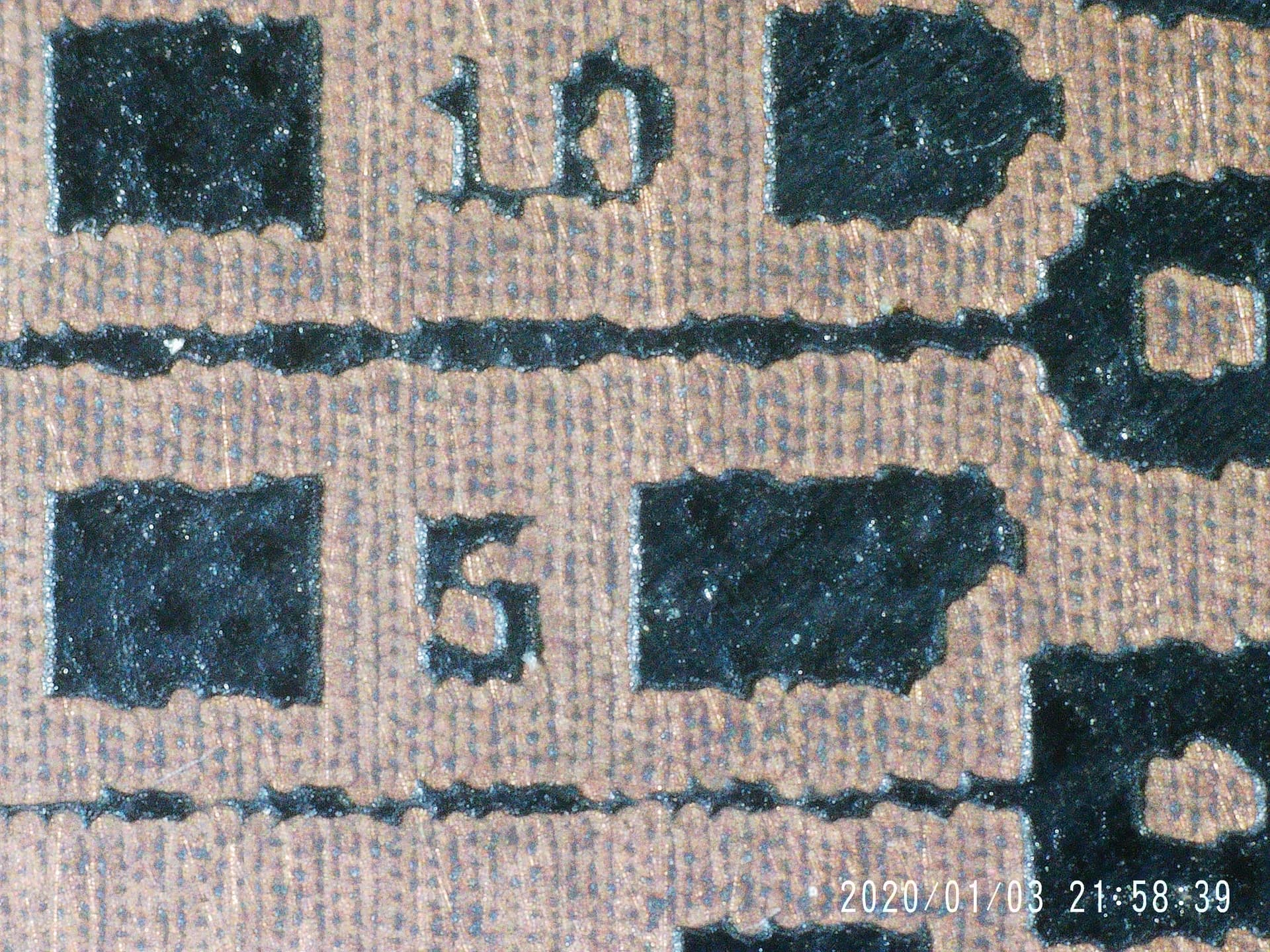
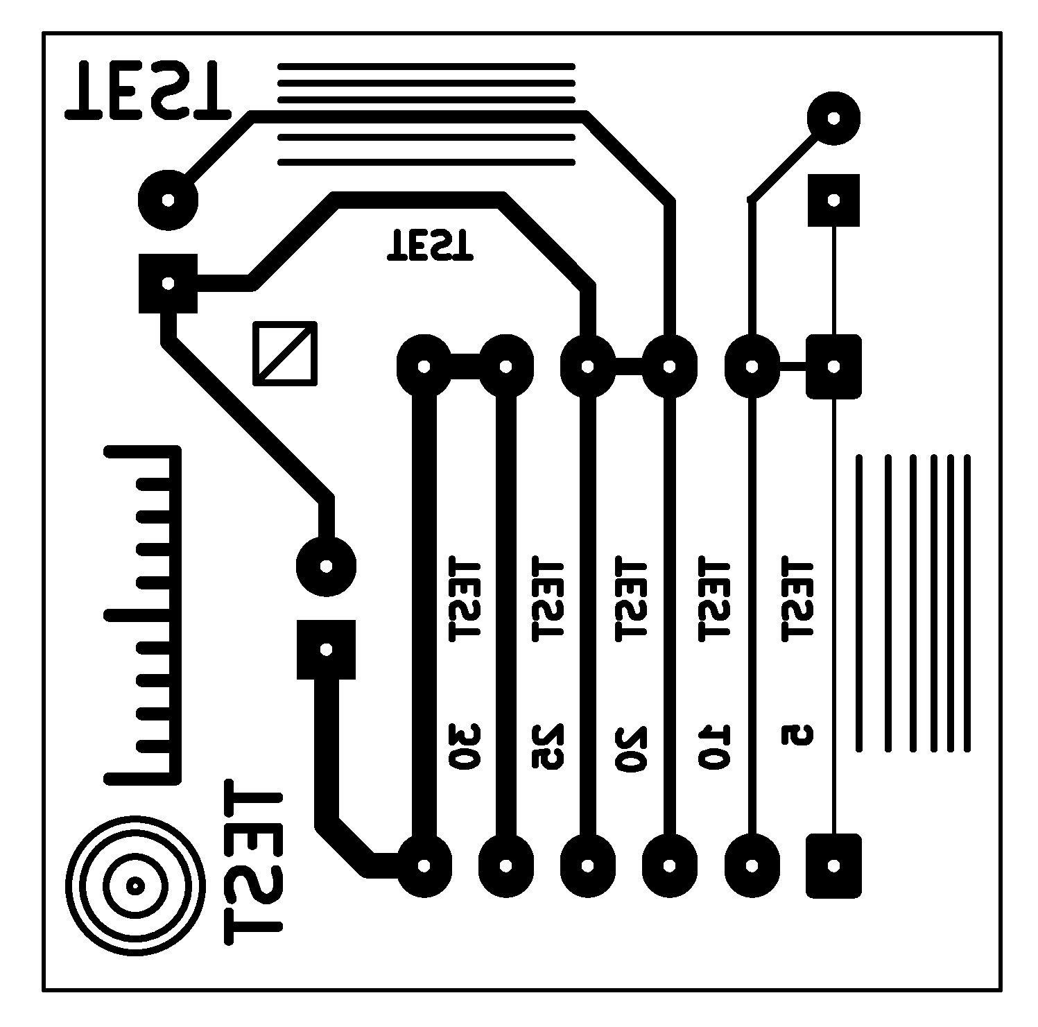
The image below shows tracks of various thickness lines from 0.12mm to thickest at the top of 0.76mm. This was done at 6800mm and 30% Power. I didnt find any improvement using pass through mode. I think I would be happy with tracks above 0.5mm as being safely engraved. Do you think there is room for improvement I think I am at the process limit for my equipment?
Thanks Best Regards Chris
1 Like
What do they look like after you etch off the unwanted copper… Probably the best test.
![]()
1 Like
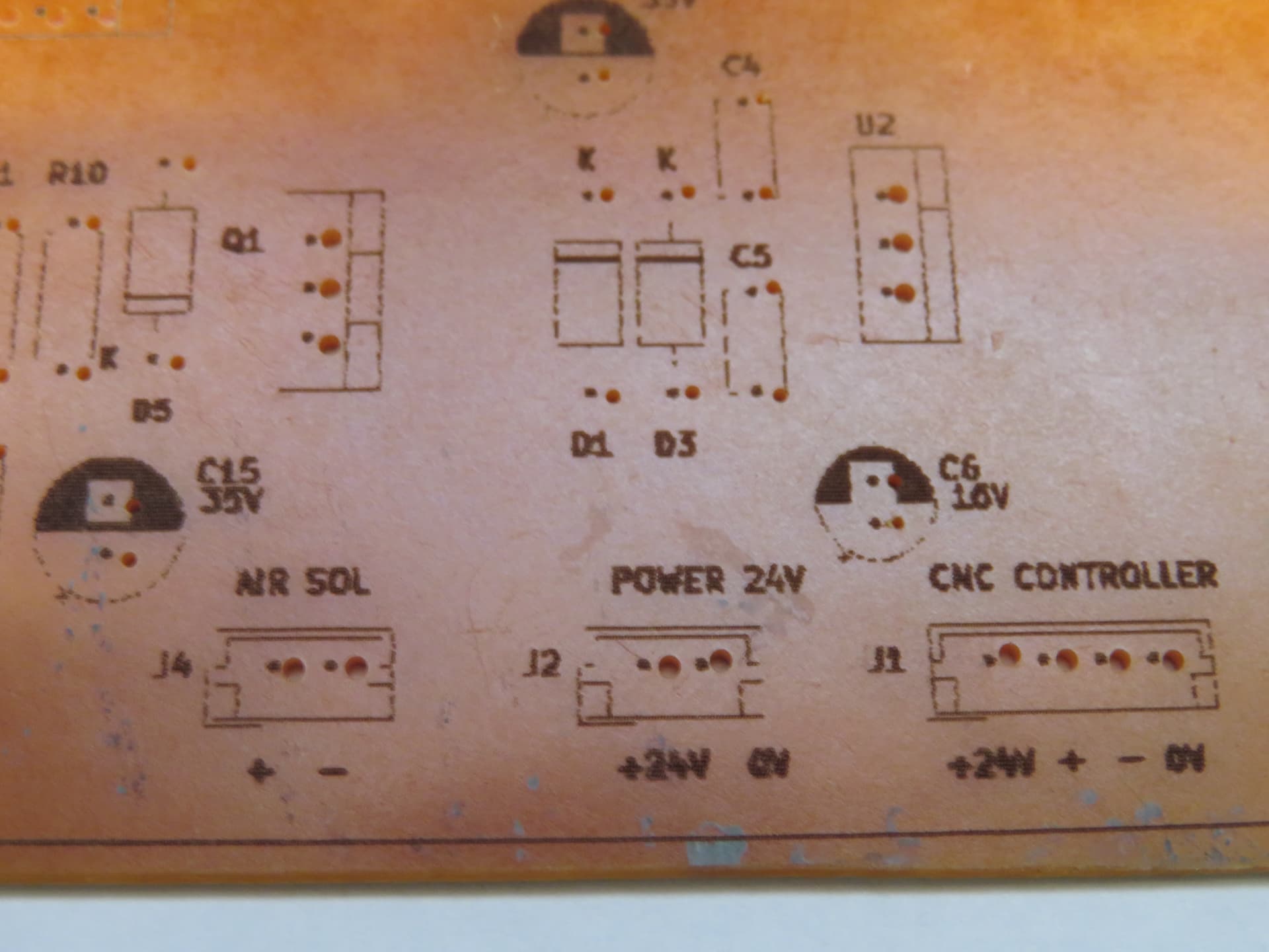
I’m going to etch my target board tomorrow which is nothing special. But I will take some pictures. I have adjusted my design so all track are above 1mm and increase clearance around the ground plane. I am confident this will work as nothing notable about the mask or etching process

For anyone interested it’s a none misting minimum quantity lubrication system for my CNC milling machine. It’s controls the air flow and doses the air with lubricant via a stepper driven peristaltic pump.
Of course! ![]()
I think engraving from the PNG image is costing resolution, but it’s hard to tell.
Steps:
- Import the 1200 DPI PNG image (post 14) into LightBurn
- Trace it and discard the image
- Rescale to the correct size
- Ungroup the trace
- Put it on a Cut layer to show the outlines
- Start the node editor to show the individual curves:

- Put it on an Engrave layer to engrave the copper areas
- Set the layer to 400 mm/s, 20% power, 0.1 mm line interval
- Engrave some acrylic:

The line interval could be a bit smaller, but IMO tracing the PNG to vectors and engraving at (almost) the machine’s ideal line interval produces better results than attempting to force-feed pixels from the PNG image directly to the laser.
The 5 mil = 0.13 mm line isn’t very good, because the laser bandwidth isn’t high enough to allow such fine detail. At 400 mm/s, that trace is only 300 µs wide but the power supply has a 1 ms response time: the tube can’t get up to full power before the pulse is over.
I also tried it with the lower-resolution PNG and got a trace with similar, slightly blockier, features. Given that you can’t import a Kicad SVG into LightBurn, a 1200 DPI PNG may be a Good Enough™ intermediate format.
This is with a CO₂ laser producing a round spot, rather than a diode laser’s rectangular spot, so your results will certainly differ!
(Now, back to what I was doing, if only I could remember what I was doing … ![]() )
)
Thanks. Quite a few steps there I’m not sure how to do yet but I will find some YouTube videos for each step. I guess I should have said is there room for any minimum effort improvement. If I can do the whole image fine but correcting individual parts of a more complicated PCB design is just going to be time consuming. I think my other consideration is going to be getting the paint off the PCB once it has been etched. I guess I will find out.
I was hoping the laser method would be a quicker method than using UV photo resist and laser printed masks. The advantage is I have no issue at 1200 DPI and can go straight to the printer. However Aligning multiple masks and messing with chemicals is also time consuming. But the UV mask method is better suited to finer detail. Watch YouTube videos looks like a fibre laser is the way to go. Unfortunately my wife will probably move out if I buy another tool.
Is this single sided?
I noticed copper pads on the surface.
How about drilling the holes?
You laser isn’t going to punch a component lead hole through the board. Some way the board has to be registered on the other machines for proper alignment.
Good luck
![]()
Drilled by hand. I think I was a bit hot and could have run the laser much faster. But I’m really happy with the first attempt. I opened up the tolerances on the board design but wouldn’t have any concern at 15mil.

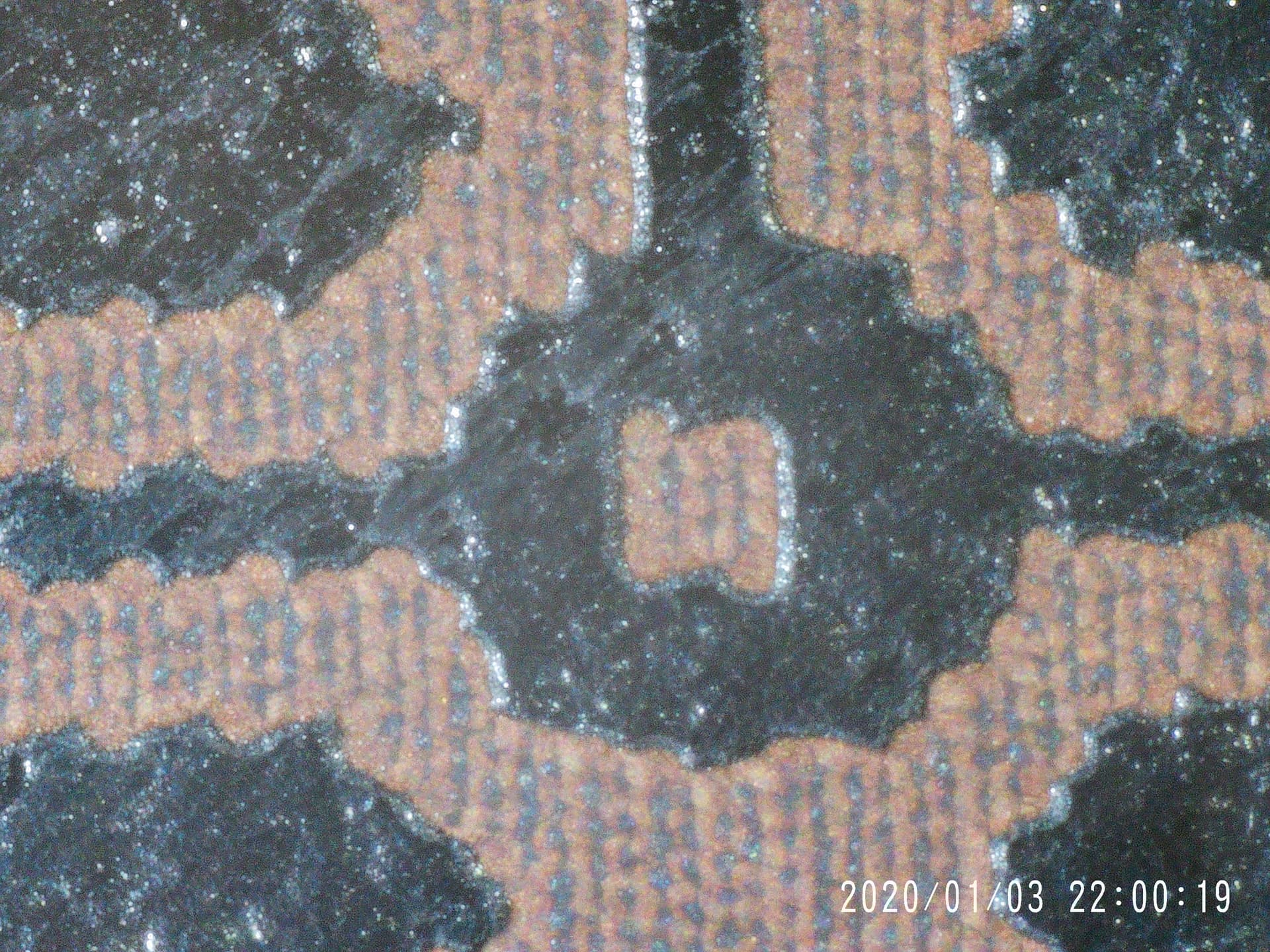
Another idea: you can also try to change the fill mode from linear fill to flood fill or offset fill, which might get rid of the pattern from many very short lines. But this depends on the spot and object width, whether it works well or not. So might not work for every trace on the board. And you need a vector graphic before, I don’t think this works with images.
Normal fill

Offset fill
As you can see here, there might be some problems of empty spots when line width and object width don’t fit perfectly…
1 Like
Thanks for all the great help and advice first class from all of you.
I am happy to have the process good enough for the manufacture of basic circuit boards. The resolution is much less then printing a photographic mask using a laser printer or using a laser printer and toner transfer method. But if all you have is a hammer this will get it done for the type of boards I make at home. My understanding is that fibre laser potentially have higher resolutions than the gantry style lasers I have employed and may be better suited for this application when small PCBs are required.
I also laser engraved the silk screen layer on the PCB top side and I think this worked out quite well for a prototype. I hadn’t planned to engrave the ident layer, so I had not considered alignment of the board when flipping it over. I did this by eye and was within about 1 mm but this could be improved with some type of fixture plate.
Next time I would increase both the text size and body to a bolder font in the future. I do wonder if there are any styles of font that would work better than others? I used phenolic material boards as I think this is a safer option and does take a mark well unlike fibre glass.
I found the whole process a bit slow with painting the mask and waiting for the paint to dry. I am sure that the speed could be much increased as you become more familiar with the process, and I think I could have run the laser speed faster at a higher power without issues.
Be nice if the laser could drill holes for the component legs but It could certainly mark the position and perhaps produce a centre punch for drill alignment. I have a small CNC router that could also drill the holes once loaded with a drill file which would be straight forward.

Sanserif = Ariel
Serif = Georgia
1 Like
This topic was automatically closed 30 days after the last reply. New replies are no longer allowed.