Lightburn VS PCB etching Tips&Tricks

Hi, I bought a fiber laser some time ago because of the increasing number of articles about PCB preparation using such a laser. I spent my vacation (two weeks) thoroughly testing this issue. Ezcad2 is already outdated and has many problems with supported formats, especially with SVG files. So I wanted to switch to Lightburn, which suits me, and I’ve been testing it for a really long time. But so far, I have not been able to prepare a PCB in either bitmap or vector mode in this software. Some parts are constantly burned through, while others are barely touched… So far, Ezcad2 works best for me personally in bitmap mode, going line by line. But I’m fed up with typing everything manually and the 32-bit limitation. That’s why I would like this post to be a kind of bible where we discuss all topics related to galvo and fiber lasers for copper processing in Lightburn. Maybe we can work out a solution or a “PCB” mode for crazy people like me.

And now for the details. Of course, I don’t know everything about lasers, but I burned through a lot of FR4 laminate in search of a solution. Looking online, most people remove most of the copper from the PCB, but I leave most of the copper for grounding or power supply purposes, so the burning applies to narrow areas between the traces.

In Lightburn, I tried all modes and mixing them. The avalanche fill works best and fastest, but areas where there is more to burn “burn” too quickly compared to the narrow areas between the abrasives. This applies to all modes for SVG files. In bitmap mode, it is difficult for me to choose the settings. If I set it too fast, it only burns the horizontal lines, ignoring the vertical ones. The pulses themselves, even though I set the pulse times, power, and speed the same as in ezcad 2, are too weak, but again, there is burning in the points where there is more to burn. It is also difficult for me to choose the dpi, which is related to the number of lines per inch. If I set it lower and slower, it goes faster, but the small abrasives burn badly and are connected. If I set it higher, the pulses are too weak (I prefer 1200 dpi). Such png files work for ezcad.

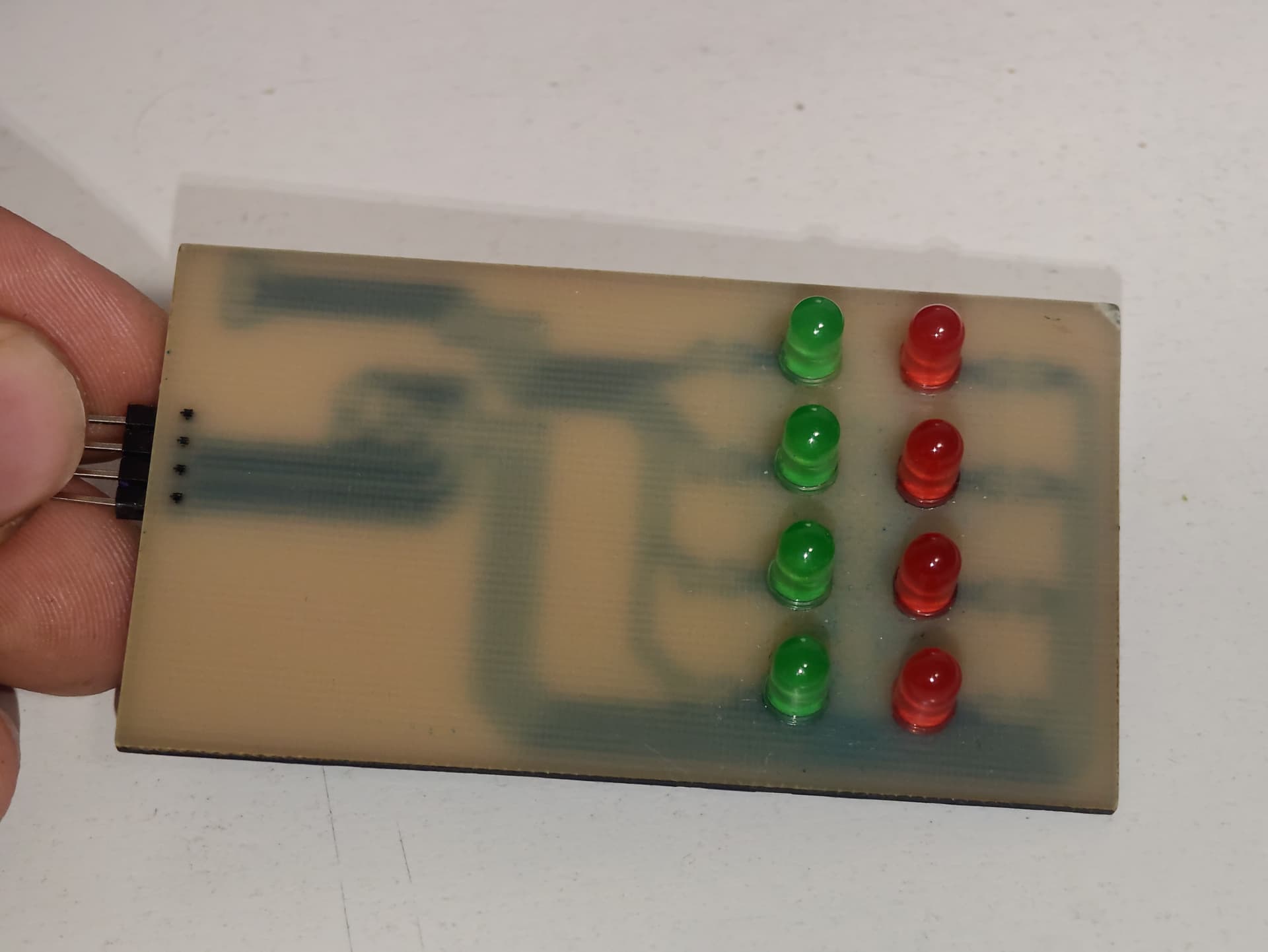
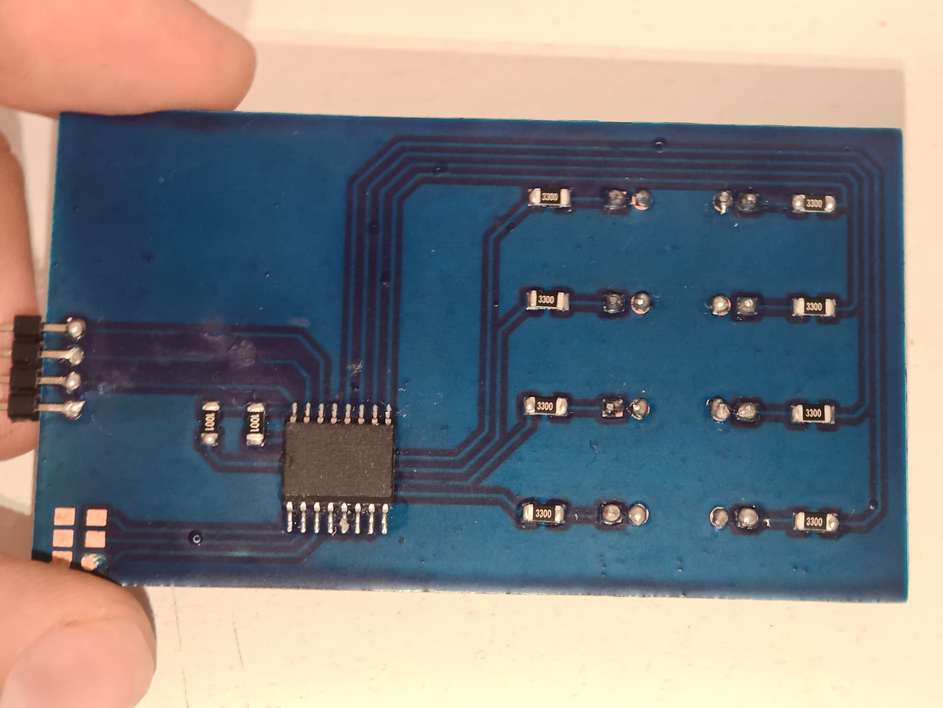
From what I have been able to determine, ezcad 2 in bitmap mode always works in a kind of “grayscale.” It is very slow, but it has a certain advantage: ezcad works line by line, and because I leave the entire background white, it causes the PCB to heat up along the entire line (by a few percent). (this apparently increases copper ablation), and even my pads with a spacing of 0.2 mm and even 0.1 mm come out okay. In addition, the pulses are stronger where they are supposed to be (I am attaching photos of the PCB from ezcad2 in “png” bitmap mode).
Ultimately, I would like Lightburn to allow for such accurate PCB manufacturing that it would no longer be a topic of “interesting facts,” because you are doing a really good job!

Hence my question to the creators and users of Lightburn: could you share your settings or contribute your description/experience to this undoubtedly phenomenal application of these devices for amateur electronics enthusiasts? My laser has an rc1001c scanning head with a 30w Raycus source and an F-210 lens with a working area of 150x150. I have also noticed that the working area is never perfect with copper, and even in my ezcad2 application, the lower areas of the working area seem to be out of focus. I calibrated the lens, the entire column, and tightened the screws with a torque wrench. I even bought a 0.5 cm steel plate to level everything, but it didn’t help (I also changed the lens and rotated it). Of course, this may be due to the scanning angle itself, because in the case of aluminum or black paper, everything is perfect, and the spirit level and caliper show that everything is ideal. Thanks for reading if you made it to the end.
Best regards.


Strona_A_Finall

Don’t have a fiber, but can I get a schematic and parts list for this project? I have a local Amateur (Ham) that wants me to experiment with UV Resist for him.

Welcome to the site :tada:


Is this a MOPA? Sounds like it from your description.


Two and a half years ago, when I got my fiber, I tried this.

Considering FR4 boards contain fiberglass, which my fiber does not cut and epoxy, which produces some unwanted gasses… and it stunk everything up… I went back to the ol cnc3018 to make them…

Biggest problem was, there was no way to make holes and everything I needed had to mount or contain feed through holes for components, even if a majority of it uses smd components.


I’d suggest you watch Laser Everything video on photo engraving. It will put an end to your interval selection issues.

We are used to lasing many things, most of which are all poor thermal conductors. The same basic issue is going to be doing this on copper… not only is it very conductive, electrically, but it’s also very conductive thermally. If you are lasing different sized areas it may effect the results.

Changes to frequency and q-pulse width would likely help. Changing lenses will change the spot size.

Something else, but I forgot… here’s a fun video anyway.

Good luck

:smiley_cat:

1 Like

Unfortunately, it’s not a MOPA laser. I would love to have a MOPA, but they are beyond my price range. It’s a Q-switched laser. Yes, copper conductivity is a pain ;_; during processing.
I watched this video and pretty much every other video on laser processing of printed circuit boards. FR4 is terrible in terms of fumes, which is why I work with two exhaust fans.
Most people use FR1, which is supposedly better because it doesn’t have fiberglass. I’ll check it out when the FR1 boards arrive. They’re hard to buy locally, so now pretty much everything is on FR4.
However, as I wrote, FR4 can also be processed without burning, as you can see in my photos above. But it takes a long time. For prototype boards, I make feedthroughs by inserting a piece of wire in the middle, which makes them practically flat, and my laser will also make the holes practically through and through, just push out the burned fragment. And that’s probably the power of the laser. To test a concept or prototype, I order boards from China after testing.
Here, for example, is the first board I managed to make with a laser (FR4 32μm of copper, single-site), nothing special, 8 LEDs and an i2c pin expander (pcf8574), but after covering it with a UV mask and curing it, it gives a really good effect at home and works.
I am also currently struggling with making double-sided tiles because aligning one side to the other is incredibly difficult, especially in ezcad2 because it does not understand the dimensions in the file metadata.


1 Like

I don’t even know if my design works. I’m getting closer, but I’m struggling with a double-sided board. If you want to test it on your laser by burning only the areas to be etched, here is a link to a simpler design. It is a board with 8 LEDs and a pcf8574 expander, which will be easier for you to test. The link contains Gerber, SVG, and bitmap files. All you need to test it is the PCF, 8 LEDs, and resistors. Resistor values should be as close to 220 ohms as possible for LEDs + 2 pull-up resistors for the I2C bus are not necessary. Additional pads for soldering to change the PCF address.

Link to my GoogleDrive: pcf_led_proj - Google Drive

Thanks, but I am not interested in actually building something like LED drivers. I was just more curious to learn the purpose of the more complex board.

I can make do with the PDF, although I will have to fix the pixellation of the diagonal lines. Thanks for sharing!

If anyone would like to test PCB burning by fiber laser , here are my parameters that work as above for ezcad2 in image mode:

Type: Image 1200dpi PNG
PCB: FR4
Speed: 867mm/s
Spot Diameter: 0.040mm
Frequency: 27.75 Khz
Power:80-95%(Finall scan 60-70)
Passes:10-30
PowerMap: defaults
I don’t use bidirectional scanning, but you can experiment.