JohnJohn
December 7, 2022, 12:06am
14
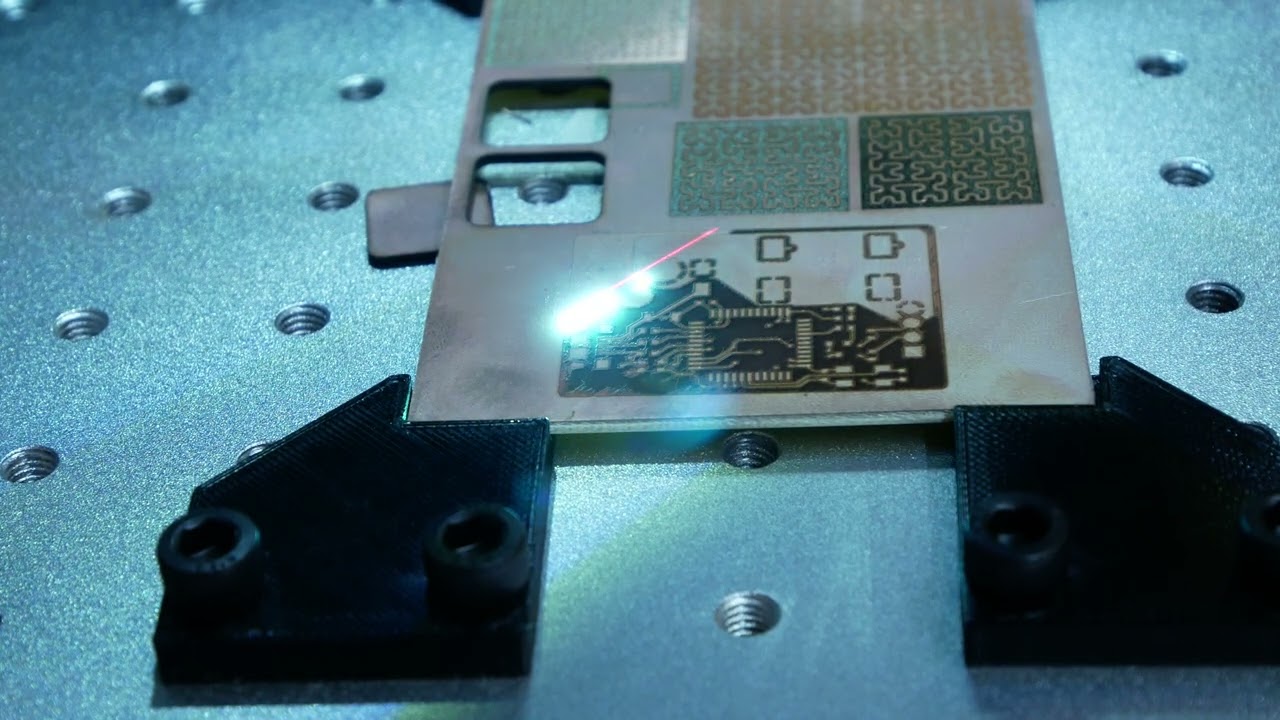
One of the devs used an RF Galvo to etch then cut-out a circuit board.
I’m not entirely certain what you mean but I can offer this terminology:
You may be experiencing something called Scanning Offset.https://docs.lightburnsoftware.com/ScanningOffsetAdjustment.html
There are also dot-width corrections for image engraving. Dot width correction?
You may even have part of both occurring here.
You can examine and confirm the GRBL parameters by requesting a report from the Console window.
The meanings of these settings and parameters are here:
## Getting Started

First, connect to Grbl using the serial terminal of your choice.

Set the baud rate  to **115200** as 8-N-1 (8-bits, no parity, and 1-stop bit.)

Once connected
 you should get the Grbl-prompt, which looks like this:

```
Grbl 1.1d ['$' for help]
```

Type $ and press enter to have Grbl print a help message. You should not see any local echo of the $ and enter. Grbl should respond with:

```
[HLP:$$ $# $G $I $N $x=val $Nx=line $J=line $SLP $C $X $H ~ ! ? ctrl-x]
```

The ‘$’-commands are Grbl system commands used to tweak the settings, view or change Grbl's states and running modes, and start a homing cycle. The last four **non**-'$' commands are realtime control commands that can be sent at anytime, no matter what Grbl is doing. These either immediately change Grbl's running behavior or immediately print a report of the important realtime data like current position (aka DRO).
show original
