At some point I want to start etching custom PCBs. My electronic tinkering is to the point where basic PCB breadboarding won’t cut it anymore. I’ve tried CNC cutting as well, but I don’t have enough mechanical (including cutting bit) precision.
The examples I’ve seen include some form of painting/coating and then engraving the area away that needs to be etched. It requires a consistent layer and thickness of paint.
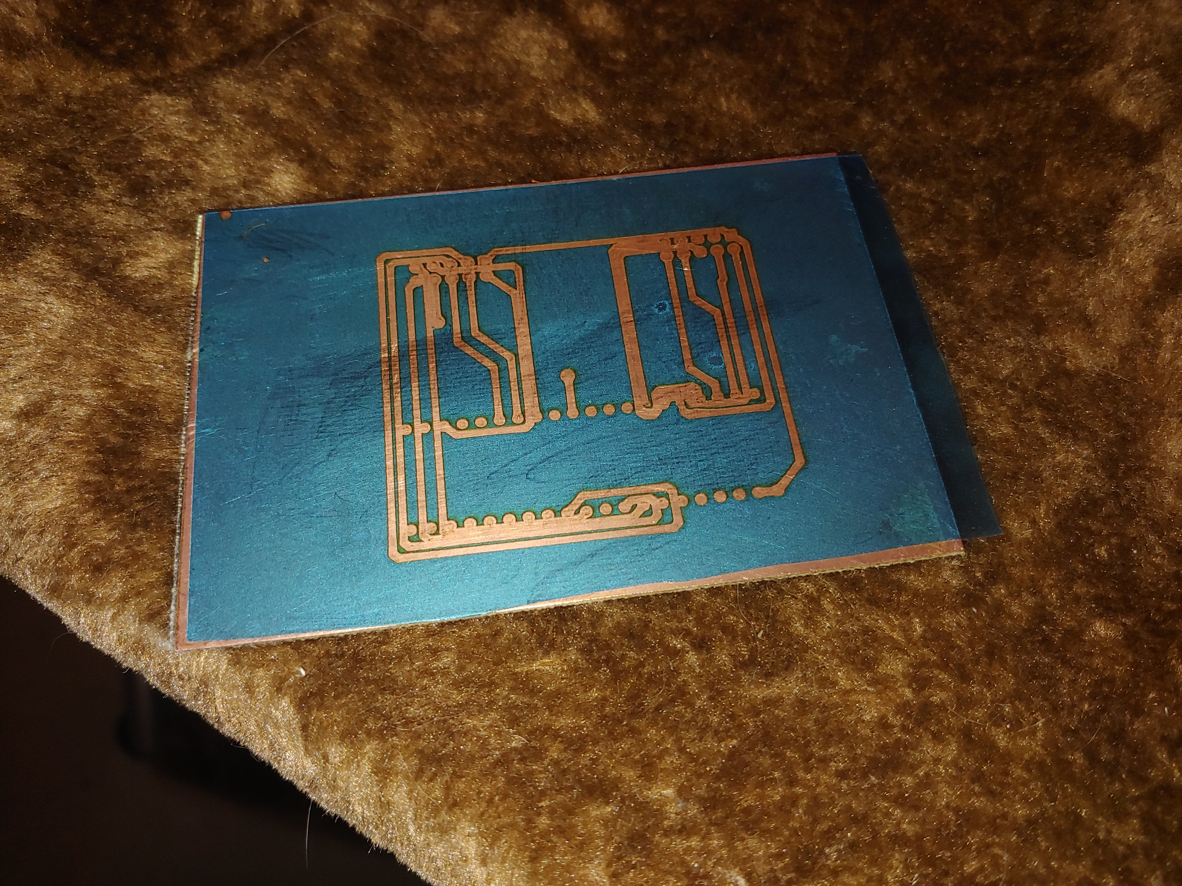
I’m trying something a little bit different. Covering the PCB with vinyl transfer tape (cellophane/packing/masking tape didn’t work). Cut way the area that won’t be etched and then paint/coat what’s left.
This is an example with fill+line. I need to redo it with a kerf, but the concept is promising. I don’t plan on spending a lot of time with it, but it might be worthwhile for others thinking about the same thing.
I’ve done a few successful boards just coating with black lacquer and lasing away what I don’t want.
I’ve also done (a lot more) boards with benchtop CNC mill and V-bits. Both techniques seem to work fine for stuff down to SOIC sized footprint or so.
Anything with REALLY small parts or if I need more than just a couple of prototypes I just send the gerbers off to the board house. It’s so much easier.
I just send the gerbers off to the board house. It’s so much easier.
I thought about that, but I’m a very iterative person. I’ll go through 3 (or 33) or so variations before I get exactly what I want. The turn-around for PCBs would still be disruptive to workflow.
Of course, I could always get better with the initial designs…