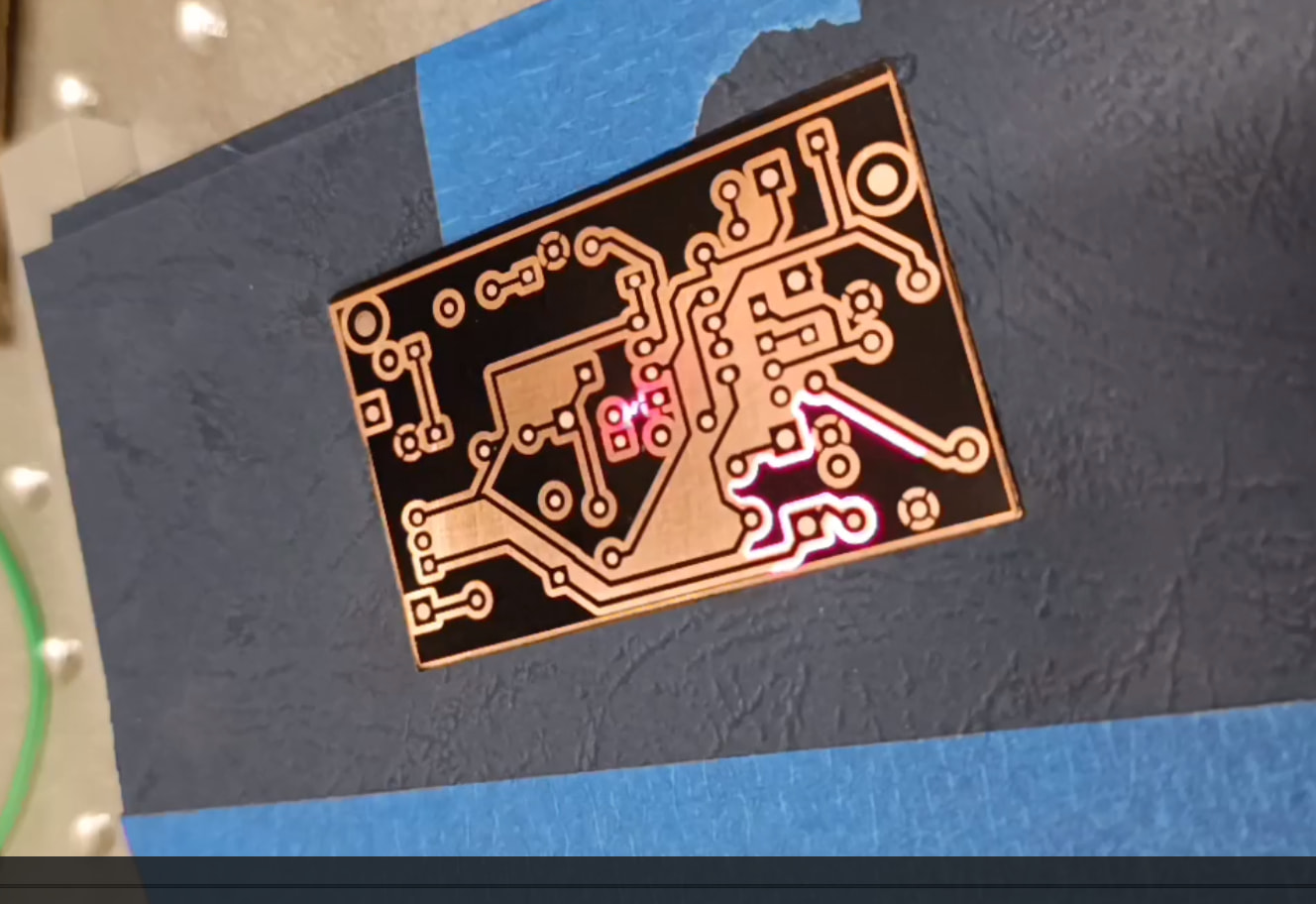
Having had excellent results with MillMage, regarding text engraving on anodized aluminum, I’m pondering what it would take to route out the the trace lines on a copper clad PCB. I see videos of people routing the copper off the board, thereby avoiding the etching process all-together. Not ready for a laser head setup just yet. Seems like routing the traces would be great for simple one-off projects. I use JLC for my multiple/complex PCB designs.
Just export the trace design as SVG and then you can use MM to remove all copper that is not needed. You might need to invert the image, depends.
You won’t be able to do it with a laser, CNC is the way to go.
There are lots of examples of this method out there. This video is about an hour and very detailed, but you can scroll to 43:30 and view the milling process.
 on a Cheap CNC Machine")
I am interested too about this experience; my results was good with laser + painted PCB and corrosion next, I was not satisfied with routing on CNC. I need more experience mainly with exact positioning for 2 faces circuit and, of course, with the design of PCB himself (pad&trace size&other).
1 Like
That is a whole new subject. When you flip the board, things not centered shift position in the XY graph.
Likely burrs along the remaining copper trace and dealing with warped boards.
I really do appreciate the input. Your experience will help me tackle the quest. Once I finish my current project of quieting down my UREI crossover for my control room monitors, I’m going to work on PCB routing.
1 Like
I have installed KiCAD on Ubuntu for PCB layout, and with the valuable help/assistance of AI I have obtained the first PCB with actual technology (first was painted by hand about 30 years ago :)). My project is stopped for a while, I hope to be back soon to improve my results.