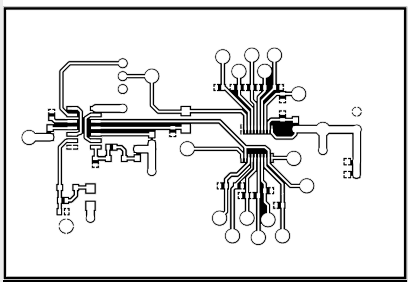
I want to create a pcb using lightburn and wanted to start off using an example from designspark. I created a reverse image pdf file which looks perfect, but when I import it to lightburn this is what I get:
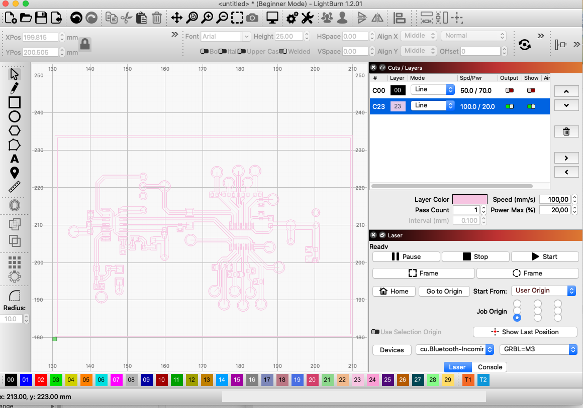
In ‘cut/layers’ I get 2 layers: C00 and C23. With ‘line’ selected I get a very dimm image, white with grey lines along the trace borders and a grey line in the center of the trace. I can barely see the traces.
When I change layer C00 to ‘Fill’, I get a reverse image with white lines along the edges of the traces and a white line in the center.
Yes it’s a recurring problem. The forum software only allows a very limited range of file types so the trick is to append ‘.txt’ to the file name (after the ‘.pdf’) and then you’ll be able to attach it.
I can create a dxf file n designspark, but it only show the holes, i.e. no traces. It does not support svg. It supports gerber, but lightburn unfortunately doesn’t.
Seems to me it’s just the layer that the pdf content that got assigned to which is hard to see. I’d suggest changing the layer to something more visible.
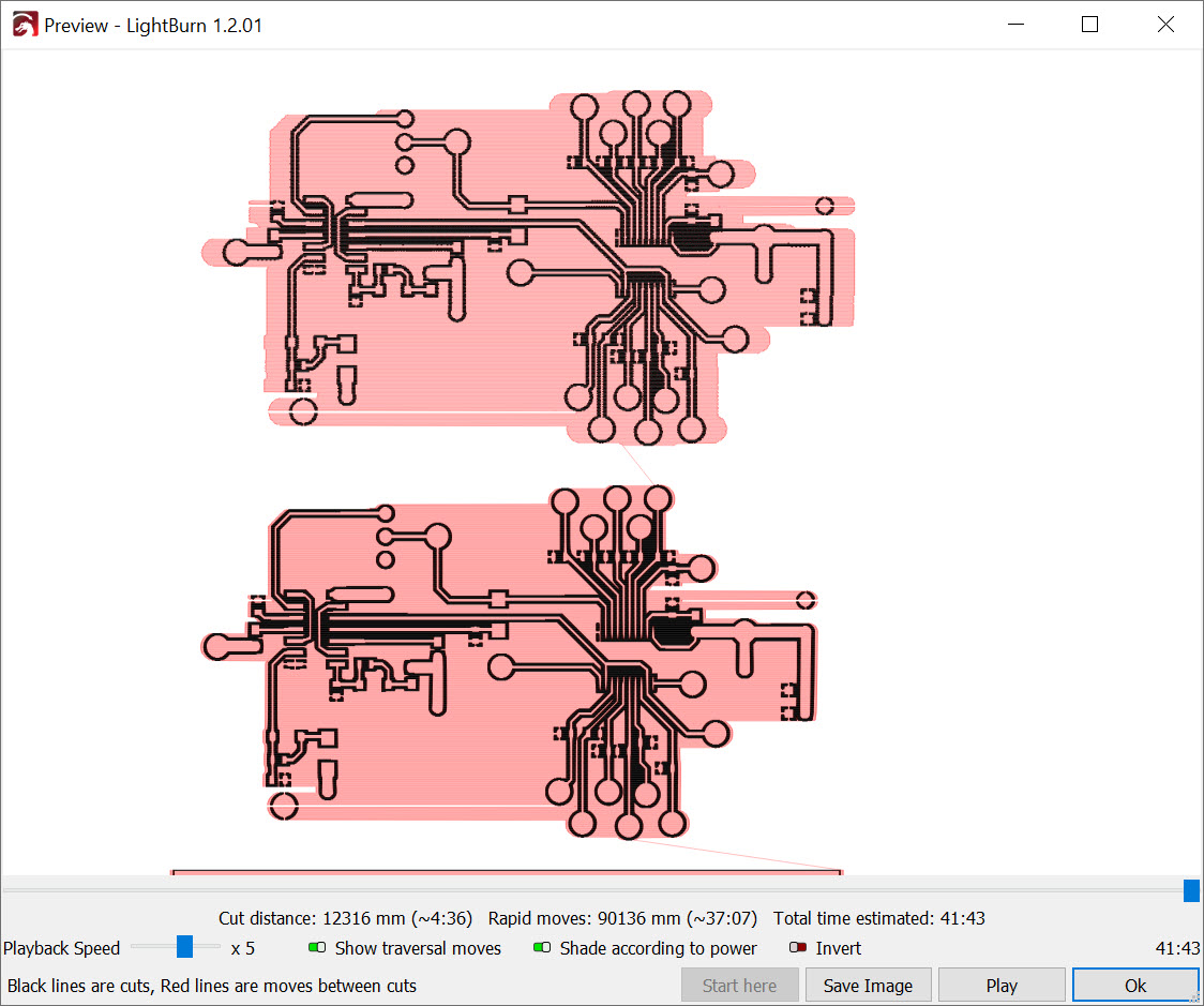
I’ve been playing around with for a while now but haven’t found a quick and easy way of getting it into LB exactly right yet. I’ve attached my attempt which is close(ish). Anyway, it’s nearly 2am here so I’m off to bed now. I’ll have another go at it later and see whether I can get it any closer.
Are you able to export from DesignSpark as a raster (.bmp, .tiff or something like that)? It won’t be as good as a vector format but it might be good enough.
Thank you so much for staying up late helping me. I really appreciate it. The lbrn2 file you sent looks good. Please let me know how you did that. Yes, designspark does support exporting .bmp, but not as a ‘manfacturing Plot’, so I don’t know if it is not as acurate. Comparing it to the lbrn2 it looks the same. I asked lightburn if they have plans supporting gerber, but they don’t.
thanks
Bent
Well, I’m not sure it’s a very practical solution and as there was a lot of trial and errorI can’t remember exactly what I did!
I opened up the pdf in CorelDraw, Affinity Designer and Inkscape to see what I was able to do in each. I ended up using Corel as I’m more familiar with it and I was able to achieve the result I was looking for. The main problem with the pdf is that the traces are described as vectors with a specific width. Unfortunately LB ignores the width and that’s why you get the thin lines instead of proper traces. I ‘Ungrouped’ everything then selected all of the traces and pads then performed a ‘Convert Outline to Object’ (there’s a similar command in Inkscape but I didn’t seem to get the same result - YMMV!).I then messed about ‘Welding’ and ‘Combining’ etc until I got something that looked right. As I said: I can’t remember everything I tried. I then used the LB macro in Corel to transfer it over to LB then move everything onto layer C00. I then had to delete a few vectors that were outlining the traces and pads. That’s about it. I’m sorry I couldn’t give you a more definitive set of instructions. I imagine with enough time and practice you could come up with a repeatable workflow to arrive at your destination every time but I’m not able to give you that I’m afraid. I’ve been messing about with it for a few more hours today but I’ve not really found a solution. I’ll probably continue playing with it for a bit to see whether I can get anywhere with it. Anyway, I’ve attached a better version. test3 copy.lbrn2 (133.5 KB)
Ok, I’ve been fiddling about a bit more, this time I think I’ve found a pretty simple way to do it. Unfortunately it uses Affinity Designer, which isn’t free but is very inexpensive and certainly a lot cheaper that CorelDraw!.
Open PDF from Designspark in Affinity Designer (I just opened page 1)
Select>Select Object>Unfilled Objects (this selects the traces)
Layer>Expand Stroke (this uses each line’s thickness and creates an outline around each trace)
Window select all the pads and traces and shift-click the copper pour
Layer>Geometry>Add (welds all the copper areas together)
Export as PDF
Import into LB
Place everything on desired layer (C00) for example
Done
It’s taken a while but it’s been interesting. I hope this helps.
Thank you for putting in the effort on this issue. I tried again using a bmp file, but it just creates abitmat of the working screen area in designspark. So the size of the image in lightburn changes depending on how much I zoomed the designspark working area. That’s of course no good.
Check your original file. I am guessing based on my experience, but I think you have multiple layers in the vector file, with some of them filled with white. I have had similar results with dark fills that were actually a white background with a black outline. I use the Pathfinder tool in Illustrator to subdivide all of the overlaps. I then remove the excess parts. Hopefully this fixes your problem. Good luck.
Your starting point should be Gerber files, not PDF. Designspark supposedly can export PCB to Gerbers.
From Gerbers you can convert directly to G-code, for example with FlatCAM (Python based, can run on Windows). Then you can run NC on LightBurn, if you wish.
Can I ask you what is your next step? I can only guess that you will burn out nitro paint and then etch exposed copper in FeCl3? Is so then g-code is identical to “isolation milling” PCB fabrication (less Z motion), should work with laser no problem.
However common PCB process is to use photo-resist that is hardened with light exposure and withstand etching, where unexposed it does not. I think photo-resist process also can be successfully implemented with laser, but there are more things to control, like proper exposure and dimmed, blue light free room.
There are much better PCB design packages than Digispark. KiCAD is fantastic, very mature today and my choice. Digispark is belong to and steering purchasing to RS Electronics. In 90s in US it was one of major component suppliers for hobbyists, competing with RadioShack, now irrelevant because superseded by Ali+Ebay+Amazon and on rare occasion Digikey, Mouser or Newark (last 3 are mostly professional suppliers). Using Digispark most likely will end up costing you more (BOM cost). But I’m sure there are ways around it.